2014-01-14

New Project: 68008 Microcomputer

Servus,

one of my weird ideas is to build a microcomputer with every CPU i own. Ok, maybe not really *every*, but some of them i memorize with nostalgia. These are:
  • Z80 with SRAM
  • Z80 with DRAM and paged memory
  • 68008, one with SRAM and one with ~ 2MB DRAM SIMMs
  • 68000, let's see
  • 68020, eventually with FPU
  • 68040, with ~ 64MB DRAM PS2-SIMMs probably
All of them will connect to the K1 Peripheral Bus, so that half of the work is already done. ;-) Beyond that, no I/O will be implemented on these boards.

You see, in essence these are two processors. I started with a ZX Spectrum and proceeded with an Atari ST before i entered the world of Apple, Linux and not Windows.

68008 SRAM Microcomputer

Let's start with the 68008. I have both, the DIL and the PLCC variant. I'll use the DIL version for the SRAM board and the PLCC version for the DRAM board, because it can address more memory: 4MB instead of 1 MB only.

The 68008-SRAM  board will the half sized – 79x100mm – pretty tight, but it will fit. The 68k CPUs are a little bit nasty to integrate into a system, because they have quite a lot of requirements, especially the 68008 which implements an asynchronous bus model. But i'll use any trick, cheat and simplification i can find to make it fit. :-)

Basic Requirements

  • 68008 PDIP CPU
  • Eprom 32 .. 256 kByte
  • SRAM 128 or 256 kByte
  • K1-Bus half-sized card

Project Page


The Board

Layout v0.1 2014-01-14
To the left is a first layout of the board with all components required for the current circuit.

The top row ICs are glue logics.
To the left is the K1-bus connector.
The circuits to the left of the CPU connect the CPU to the bus.
The two 74HC573 registers expand the 8 bit bus of the 68008 to the 8 or 16 bit K1-bus.
The 74HC367 hex driver plus some resistors implements the i2c interface.
The 74HC138 decodes the strobe signals for the K1-bus.
In the center of the board is the CPU
and right of it the SRAM and the Eprom.


Requirements and Simplifications

• Memory Map. Memory is divided into 4 sections: RAM, ROM, fast I/O and slow I/O each of which is 256 kByte in size. This limits the size of the RAM and Eprom.

• CPU Clock. This is generated by a 10 MHz clock module. I avoid the hassle of generating the clock signal "by hand" with a quartz and inverters.

• CPU Reset. The 68000 family needs 0.1s low on Reset and on Halt for power-up initialization. This is currently done with some R and C and a Schmitt Trigger inverter.

• CPU DTACK. The 68008 needs an acknowledge for every memory read or write access. By delaying this signal you can add wait cycles. By never asserting this signal you can make the CPU hang for ever. This signal will be handled in the most simple way possible: It is tied to ground and this way always asserted. According to some other 68008 projects, where they do this for the test run on a bread board, this should work. Drawback: No wait cycles possible. I'll need a reasonably fast Eprom and SRAM. This also applies to the fast I/O.

• Bus Error. DTACK is always asserted and BERR is tied to Vcc. There will never be a bus error.

• Bus arbitration. The K1-bus does not support multiple bus masters and so does this board: bus request BR and bus grant BG are not used.

• Interrupt control. The 68008 PDIP has two interrupt input lines which can encode 4 states: no interrupt, 2 normal, prioritized interrupts and a non maskable interrupt. The only source for interrupts on this board is the K1-bus and so i need only one normal interrupt. The K1-bus supports prioritized interrupts by enabling/disabling interrupts directly on the attached extension cards.
Now the nasty thing: Devices must provide an interrupt vector during the interrupt acknowledge cycle. An automatic vector can be requested by asserting VPA and so we need to know when a bus cycle is an interrupt acknowledge cycle. For this we must decode the Function Code outputs FC0, 1 and 2 which are all '1' during an interrupt acknowledge bus cycle.

• K1-bus access. As said above there are two address ranges for the K1-bus: fast and slow.
The idea is to use a standard memory cycle for fast I/O where wait cycles are not supported because DTACK is permanently asserted. This is suitable for very fast peripheral cards and for switching interrupts and i2c on the K1-bus.
For slow devices i want to use 6800 peripheral I/O cycles by asserting VPA (valid peripheral address) in this address range. This will do a bus cycle synchronized with the free-running E output of the CPU (which has a fixed period of 10 CPU clock cycles) with at least 11 and at most 18 CPU clock cycles due to synchronizing; and no wait states because of the fixed alignment to the E signal. Eventually i'll come up with something better here.

• CPU VPA. This input was already discussed in two requirements above: Interrupt control and K1-bus slow access. During an interrupt acknowledge cycle it is pulled low to request an automatic vector (interrupt routine start address) and in slow I/O it is pulled low to request a slow 6800 peripheral bus cycle.

• K1-bus 16-bit I/O. Peripherals on the K1-bus may use 16 bit I/O. The 68008 has only an 8 bit data bus. There are two possibilities: I use it 'as is' and attach only 8-bit extension cards. Or i add 2 latches to store and receive the upper byte during a 16 bit I/O. I have some K1-bus cards which use the 16 bit bus, most namely the IDE board because IDE is 16 bit wide, and so i'll invest in two '573 data latches.

• K1-bus i2c. Peripheral cards on the K1-bus can have i2c EEproms to signal presence of and identify the card and to provide a universal byte-coded drivers. This costs one '367 hex driver IC plus some resistors. This makes it possible to add arbitrary cards to the microcomputer.

• ROM and RAM. The EPROM and the SRAM may be up to 256 kByte in size each. Due to space constraints only one SRAM IC is possible. Memory access cycles of the CPU are without wait states (see DTACK above) and therefore the memory ICs must be fast enough: Scrutinizing the bus cycle timing charts i expect that 150 ns access time will do it; eventually up to 200 ns will work.

• System Timer. There is no system timer on the board. Instead it is expected that one of the K1-bus cards supplies one. This is fairly easy, because my serial cards with one (or more) 88C192 dual UARTs can supply this.

• Serial and Parallel Ports. Any connection to the outer world requires a K1-bus extension card.

2013-02-03

Version 1.0 of i2c driver EEprom specification


Hello,

Version 1.0 of the specification for the driver i2c Eproms on the peripheral cards is finished.

I have also finished translation of the K1-Bus documentation, which was initially written in German.

Here are the links:

K1-Bus documentation: http://k1.spdns.de/.../K1-Bus/
Driver EEprom layout and bytecode: http://k1.spdns.de/.../K1-Bus/i2c-eeprom.pdf

    ... Kio !

2013-01-21

K1 Bus Update

Hello,

after i have worked for some months on my ZX Spectrum emulator, i'm now back for a while to the K1 CPU.

I worked on the draft for the driver i2c eeproms on the peripherial cards. They are going to version 1.0 soon. In the course i've started translating the K1 bus documentation, which was initially written in German. There is quite a lot of text to translate.

If you are interested, here are some links:

K1 bus documentation: http://k1.spdns.de/.../K1-Bus/
Driver eeprom layout and bytecode: http://k1.spdns.de/.../K1-Bus/i2c-eeprom.pdf

2012-07-18

XVGA TFT update

Hello,
i made some progress with the XVGA controller board.

Current State of the Board

First, it becomes more expensive, because it had to buy a minimum of 5 of the FPD-Link transmitter chips (note: i sell the others. Interested? ;-). Then the layout is very tight. See here:
2012-07-18 autorouted board
ICs placement is nearly final, then i'll add some more hand-routed wires, auto-route again and then hand-optimize. This will take a week or two.
I had real problems with the rams and FPD-link controller, they actually just fit between the '245 bus transceivers and the VGA connector. I tested a couple of arangements, but this produced the least vias.
FYI: bottom left is the 16 bit K1 bus, directly above two 74245 bus transceivers, the SMD ICs are RAM and the FPD-Link transmitter. 6 chips next to the right are drivers and drivers with latches, which are used to select between an externally supplied address (for the CPU reading/writing the video RAM) or internal address from the counter cascade, used to address the video RAM for display. Next 'column' of chips are the external address registers/counters, next are the internal address counter cascade, the vertical chips at the right are clock and ATtiny. Bottom right 6 ICs are the control logic. There's an I2C EEPROM sitting on the rear side of the PCB underneath the bus connector.
Though i us a 15-pin VGA SUB-D connector, the signal is not VGA but transmits 4 LVDS signal lanes, each 3 wires: pos. and neg. differental signals and associated GND. In addition one PWM signal is transmitted on pin 15 which will control the LCD backlight brightnes. According to what i found in the net this is a 5V 125kHz PWM signal.

Current Circuit

Here's an update to the circuit as well:
Circuit 2012-07-18 - Data Paths

Circuit 2012-07-18 - Control Logics


2012-07-04

XVGA TFT

Though i should finish the built LCDs first, i've already begun with 3rd display. I's a 1024x768 pixel TFT from my old iBook. It has a LVDS FPD-Link connection and i have searched the web for info about the panel and FPD-Link. I think i've got enough info to build it.

Major problems:

I need a special transmitter chip, preferably in 5V. These chips are generally hard to find (never used by hobbyists) and 5V is even harder. But i'll get a quote today. :-)
Timing is at the upper end of any hobbyists project: Pixel clock is 65 MHz, may be eventually lowered down to ~62 MHz.
This requires at least 15ns RAM, which will result in very tight timing, or better 12ns. And i need 1.5 MByte of it. Though i have plenty of RAM in stock, i opted to buy three 256Kx16Bit 12ns RAMs. Head count of ICs on the PCB is already very high.

Data flow on the XVGA controller
Control signals

Project Page

The project page is .../IO-Boards/VGA/ on my home site. This is on my private computer and everything i do here is directly visible on this page. Currently it contains a collection of spec sheets and the current state of the controller board design.


The Plan

The design ideas are as follows:
• The VRAM is addressed by a 20 bit counter cascade. Due to timing problems, the address is buffered by a set of 74574 latches, so the address is always one clock cycle delayed. The RAM output data is directly fed into the FPD-Link transmitter, which is clocked by the same clock signal. All running on 64MHz with a clock cycle of ~15ns.
• The slow signals, VSYNC, HSYNC and DE (Display Enable) are generated by an ATtiny. It also controls count enable of the address counters, to stop them during HSYNC and VSYNC (or, when DE is false). The ATtiny will be clocked with 16 MHz synchronously with the 64MHz pixel clock.
The ATtiny will also generate the FFB (frame fly back) interrupt signal, which is very important:
• VRAM access from the CPU will be completely asynchronously with the pixel access for the display. It will simply override the signals for the display, resulting in 'snow'. Each access will 'destroy' the display of approx. 3 pixels. This allows me accessing the VRAM without asserting the !WAIT signal on the bus. I have already checked the timing, writing is safe, reading is tight, but should work.
Accessing the VRAM requires sending an address and then one data i/o. The address is 20 bit, so it has to be transferred in two chunks. I opted to split the address in two 10 bit packages, which will directly translate into X and Y pixel address. To reduce the required bus transfers, i designed the address registers as counters as well. They will provide an auto-increment feature, so that i only need to set the start address and then can read or write in burst mode, hopefully with the full bandwidth of the bus of 16Mwords/sec. The X address can auto-increment, the Y address can auto-decrement as well. I probably can't make the X address easily auto-decrement, because i simply have not enough control lines to control this easily. The 'control lines' are the bus's address lines, and it has 6 of them.
To avoid the 'snow' effect when accessing the VRAM, i plan to do most i/o during the vertical frame flyback, which may be up to 10% of the total frame time. The exact maximum number of lines during ffb of my display will be determined when it is all built, therefore it's nice to have it programmable, because it's done by the ATtiny. It will be slightly tricky to align the control signals of the ATtiny with the 4-pixel boundary (ATtiny clock is Pixel clock ÷ 4) because the DE (display enable) signal for the FPD transmitter and the count enable signal for the address counter must not start and stop somewhere in the middle of a 4-pixel package but exactly at the start or end. Else the image on the TFT will be shifted some pixels, missing some at the left side and displaying garbage at the right side.

Let's see how it all works!

2012-06-27

The K1-16/16 CPU

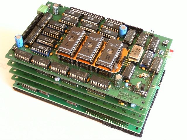
The self-built K1-16/16 CPU, built with standard 74xx CMOS ICs

The K1-16/16 CPU is the heart of the self-designed and home-built K1-16/16 Computer.
It is built with CMOS ICs from the 74AC series and fits on 5 Euro boards (160 x 100 mm).

Sometimes you are struck by an idea...

Due to depressions programming became harder and harder. So i thought, why don't do something more simple, with more manual work? Electronics, for instance. And, thanks to the internet, i have already read from other maniacs, who built a 6502 CPU. Or a Z80 in FPGA. Or Dennis Kuschel's myCPU. And there's a web ring about it. If others can do this, it can't be that hard. Basically...
Of course my CPU should be Different. Better. And Simple, so that i can understand it myself. B-)
For symmetry i settled with a 16/16 bit design: 16 data bits and 16 address bits.

Unusual and Generally Interesting Parameters

• Combined Harvard and Von Neumann architecture
• 16 MHz system clock
  Front panel with slow motion clock for exhibitions et. al.
  Full static design down to 0 Hz
• 16 bit internal data bus
• 16 bit internal address bus
• 64k x 16 bit internal ram
• 32k x 24 bit microcode
  organized as 2 code planes à 16k for conditional execution and branching.
  the microcode is copied from eproms to rams during boot for increased speed.
  it is also possible to load the microcode from an external source instead.
  the microcode implements:
    boot code, BIOS, kernel
    100++ assembler opcodes for ram-based programs
    100++ millicode opcodes for microcode-based forth or c-style programs
• No flag register. (but flags)
• Built with discrete logics using 74HCxx and 74ACxx ICs
  CPU fits on 5 "Euro" printed circuit boards (160 x 100mm)
• Manual circuit design
  Manual routing of the PCBs (with EagleCAD)
  Professional made double-layer circuit boards

Harvard Architecture 

Programs can be written directly in microcode. Adopting this view, the K1 CPU has separated program and data memory. This is the Harvard Architecture.

Von Neumann Architecture

More likely, the CPU can also use a fixed microcode, which reads opcodes from the ram and executes them. Seen this way it has a combined program and data memory. This is the Von Neumann Architecture.

Start on blogger.com

Hello,
I'm building a CPU for 4 years now (more or less) and accompanied this on my home page k1.spdns.de. This worked quite well but i wanted to separate the blog from the project documentation itself and i wanted to enable some feed back. So i started this blog on blogger.com. I will move some stuff in here which previously was on my website; i'll see whether i can fix the dates.

     ... Kio !

2012-06-12

2nd Display

Going into mass production. ;-) I built a second, very similar LCD display which uses the same controller board. This one has a backlight, but it was CCFL. I had no inverter and building one and adapting it to the CCFL wold have taken too long and so i replaced it with an array of LEDs. Not good but working. See the photos on the LM64K101 - LCD Display 640x480 project page. Next is to debug the terminal software a little bit more and use it as output for the computer.

2012-05-26

Debugging the LCD Display Driver and Hardware


This week i worked on the 640x480 pixel b&w LCD terminal.  Soldering was easy, but fixing all the bugs took some time. I also had  to do some changes to the terminal code because i realized that i was using the LCD upside down.

I connected the LCD and powered the board through the programming  header. Off course nothing worked, except for the display refresh routine, which brought up a picture of the erased DRAM cells. Step by  step i brought up more functions: Erase screen, print characters, read  and write whole pixel lines and scrolling. I had to add some nops to the DRAM read and write timing, because the data goes through series resistors which create some delay. For the next board i'll reduce them slightly. Then printing of standard-size characters with 4 attributes in all combinations works.

 Finally one last important step: Attach it via serial line to USB to my Mac. Nothing worked. I adjusted the Baudrate on both sides. I printed text from the LCD terminal on the serial line in an endless loop. There was no signal on the TxD line. Why? But there seemed to be a signal on the RxD handshake line. ... ???

I had connected data lines to handshake and handshake to data lines on the board. :-(. Fixed it with a cutter, solder and wire. Tested. Worked. :-)

2012-05-19

Debugging i2c


And on it goes. The last days i spent finding out, why the i2c interface did not work. Hardware is ok, it's a problem with the software. First i thought, all i2c eeproms have a block size of 64 bytes. But that's not that easy. Block size varies with eeprom size. And manufacturer… :-| But most 8k eeproms have blocks of 32 bytes and most 16k and 32k eeproms have blocks of 64 bytes.

Then busy polling after a block write did not work properly. I started a read cycle to detect the busy state (the eeprom does not respond if busy) but this behaviour is only defined if you start a write cycle. So i rewrote my source to do this.

Then somehow my start and stop sequences on the i2c bus sometimes failed. Now i test-read the data line to see if it is high and not pulled low by the target, for whatever reason.

Now access to the K1 bus eeproms works properly and hopefully reliably. I successfully downloaded the SIO driver code into the SIO driver eeprom and booted the CPU with driver initialization from eeproms, and not with data from the microcode. And it works! :-)

And, last not least, selecting the i2c eeprom on a K1 bus card works as planned: All eeproms are addressed with address 0b000, but only the eeprom on the currently selected extension card actually has this address. The i/o cards disable their eeprom while they are not selected, and the easiest way to do this is to set any address pin of the eeprom to '1', so that the address does not match.

2012-05-14

Debugging the SIO board


Instead of writing some 'useful' commands i spend the last days tracking down a weird error. When i activated the timer interrupt of the 88C192 UART to give me a system timer interrupt of 100 Hz, the whole system got stuck. The simulator worked, the real hardware stalled. Bad!

It took me some time with the minimalistic debugging facilities to come to the conclusion, that the interrupt does not go away. When i rewrote the RETI (return-from-interrupt) opcode to execute the next  opcode regardless of interrupt state the system made it to the shell prompt, though eating all the cpu power. This only happened when i enabled the timer interrupt, else everything seemed to be ok. I double checked my code three times. Have i a broken UART? Is the documentation wrong?
Finally, when i programmed the UART to the longest possible duration, this left ~90% cpu time in the 'Halt' state (at 8MHz). Some observations later i discovered, that interrupts came in bursts. I measured the burst rate: ~3.5Hz. I did a calculation of the interrupt frequency: 7.372MHz/32/0xFFFF = 3.515Hz. This proved, that the timer interrupt generated the bursts.

But why did the interrupt stay active for ~1/35 sec (given the 10% cpu usage) and then go away? I examined my circuit design very carefully ... VERY carefully ... this whole thing looke like a ... and there i got it: The /INT output of the UART is open collector and i had no pull-up resistor fitted there! Now all observations made sense. I soldered a 5kΩ resistor between 2 suiting pins, restored the SIO eeprom driver, compiled the microcode rom, uploaded it to the front panel, resetted the cpu from the front panel eeproms and yepp, it worked! :-) The timer interrupt now eats approx. 1% (at 8MHz).

2012-05-02

Debugging the CPU

2012-05-02

I'm now moving back from emulation to the real hardware. I expected problems, and there they are.
Somehow upload of microcode files to the front panel did not work. First it hangs with XOFF, so i disable XON/XOFF and lower the baud rate. Then it transfers up to address 0x4A00 and aborts with an error. Each time i try to do 'something' to find out the cause the error changes. Finally i find out that at that position is the first unused gap in the microcode and obviously refresehing the LCD is so time consuming that even the longest delay after one line of code (100ms) is not enough. Strange, when i re-enabled XON/XOFF it worked. So microcode upload to the CPU is working again.
Fundamental Timing of the K1-16/16 CPU
Now the code does not make it beyond the initial register test. Loading the SR (shift-right) register failed to load the CY input to data bit D15. I remember that there was a problem with exactly this when i tested it more than one year ago. I had settled my mind it was a contact issue and tried to prove this now again. But it isn't. Actually the little chart with the fundamental timing of the CPU contains the secret:
The blue clk is the load signal for the registers – SR is a register – and the rising edge is where it latches new data from the data bus and, in case of data bit D15, from the CY line. The CY line is a 'option control' line, it controls options in the various registers, if they have. As can be seen in the image the option control line toggles exactly at the same moment (if it toggles) when the clk line raises. So we have a race condition here.
The only thing i can do is to delay the CY option control line for the shift registers. I examined whether this problem will show up at other places too, but it seems not. Whereever CY (or any other option control line) is used, there are some gate delays between the option control line and the data latching register. So it's enough to delay this signal for SR and SL only. Luckily there is an unused OR gate on the data registers board which i will use for this.

2012-05-03

All test code performed without error. :-) Except for i2c test, because i have not yet attached any io device.

2012-05-04

Weekend … phantastic weather … what to do? ok, i manufactured the K1-system-bus. ;-)

2012-05-05

Tata! The SIO board works. Today i got the console prompt on the terminal. There are still some issues to examine: Speaking to the i2c eeprom did not work. The hardware seems to work properly, but the eeprom does not respond. This is to be investigated. Whether interrupts work as expected is still to be tested. Though they seem to work.

2012-05-06

Yep. Interrupts obviously work. SIO works: i/o to serial to my Mac works and i/o to the front panel works. Now i'll have to add some extras to the terminal in the frontpanel, e.g. handle some control codes. ;-) And then add some stuff to the boot shell of the computer, like cd, ls and so on. And investigate the i2c problem.

2012-03-26

SIO, IDE and Terminal

2012-03:

SIO board
I have used the wrong SO-8 package in the drawings for the SIO and IDE board and had to place the I2C EEprom very carefully on the PCB to solder it. The pins extended beyond the solder pads, but it seemed to work.

2012-03-17: Heart attack: i took a look at the 88C192 SIO's PDF and saw that pins were numbered starting at a corner. X-( .... but this was for the TQFP-44 package only. Pin numbers of the PLCC package start in the middle of one side. HTF were these brain dead idiots... ?


IDE board
Soldering the 50 CF card adapter pins went quite well: Some flux applied in advance, soldering the pins with as little tin as possible, ignoring all junctions and blobs of tin and then removing most of the solder tin with desoldering wick. perfect. Stacking of the CF card and an IDE Flash drive works as desired.
LCD driver board
I hope everything will work. Testing starts ... soon. :-]
 2012-03-26: The PCB for the above mentioned LCD display project arrived. Yet another board to test and to write software for. But this one is easier.

2012-02-22

SIO and IDE Cards


After a long time where i played around with the C-style compiler for the microcode, which i expanded to a virtual instruction code compiler for use on my Mac, i resumed work on the half-sized IDE interface and the half-sized serial adapter. The IDE interface will connect two devices, a 96 MB DiskOnModule with a 40 pin IDE connector and a CF adapter for removable drives. The serial adapter will only be used temporarily for the K1-CPU itself. It will be replaced by a 4 channel (or evtl. more) serial card later which will also incorporate a LAN adapter module, which i own. The serial ports can be used for asynchronous communication with SW or HW handshake or with clock signals of any polarity. XOR gates are useful programmable inverters. ;-) The 88C192 chips have idiotic restrictions for the selectable bit rates. :-|
The two boards have been ordered on 2012-02-04 from Leiton, like the others.
Related to the CPU project is another project which i was working upon the last two weeks: A controller board for an old black&white reflective LCDisplay i own. It is based on an ATMega8 and uses old 41464 DRAM chips for it's frame buffer.
20212-02-22: The IDE and SIO boards arrived. I got two of each, due to overproduction, for fair additional costs. But the boards don't look good this time. Like processed in over-aged chemicals or the like. I don't know.

2011-07-15

Serial and IDE Cards

Currently i'm working on the microcode again. I reworked the existing c-code to match the new compiler and started work on device drivers and file system. Some peculiarities were introduced due to the pure 16 bit design of the CPU.
Also, i started the design of a half-sized serial card for the K1 bus and a half sized IDE card. When these are built i can restart working with the real CPU. But i'll probably test them in the emulator first. For the IDE card i have the choice to use a 96MB 40-pin IDE flash rom module or a compact flash adapter. Combining them may be a little bit tricky because IDE uses TTL levels and compact flash CMOS levels.
For the serial card i'm using an 88C192 which can also provide a regular system timer interrupt.

2011-04-15

Vicci 's got a name


The last months i was busy rewriting the compiler in C++. Meanwhile it evolved into a fully fledged compiler/linker/virtual code interpreter for i386/i386x64/ppc. Now most things work and i'm starting work on the K1-CPU [microcode] assembler backend.


2010-07-15

Reworking the assembler


I'm in rehabilitation after the operation. I use the spare time to rework the microcode assembler. It was a 2-pass assembler with a not-so-good approach for code placement (fitting). Now it is a single-pass assembler which is faster in most cases and much faster in all others and which tiles the microcode 'threads' much better than before.

2010-06-27

In Hospital

2010-06-22 – 2010-06-08

In hospital for operation of my herniated disk. After back pains suddenly disapeared one month ago i developped paralysis of some muscles in the left leg.

2010-06-27

A good friend of mine died unexpectedly.
Rest in Peace, Gômmel.

2010-06-15

New: a c-style compiler


The zoo of programs became an additional member: a c-style compiler. Internally it generates an 'intermediate' instruction format which is converted by an 'assembler' step into assembler opcodes which the microcode assembler understands. Later the assembler step will be replaced by an opcode assembler to create ram-loadable programs. The compiler will take some while to debug...

2010-05-31

Short Survey on Programs

The microcode software is under development. I'm juggling with 5 or 6 types oft software:
- microcode
- millicode (yes, that's new!)
- bytecode (new too)
- assembler opcodes in ram
- the microcode assembler
- the microcode emulator (new)
- vipsi script interpreter (found the second bug in it after 5 years) B-)
So, slowly, what are they all about?

Vipsi Script Interpreter

The thing of software which also delivers this web site. The microcode assembler and the microcode emulator are written in this script language too.

Microcode

That's obvious, hopefully. The codes actually executed by the control unit. All living starts here. After reset it also is obligued to setup the machine and load drivers and program. There are no other roms in the CPU: the microcode also contains the BIOS.

Assembler Opcodes

That's what the microcode is going to implement: Opcodes for a program running in ram. All opcodes are actually addresses of tiny programs in the microcode rom which load the next opcode when they are done:
:ADD ( a b -- c )
    add (hp--)
    jp  (ip++)

Microcode Assembler

The piece of software which reads the microcode sources and creates the hex files for downloading into the microcode roms. It eases my live with flow control instructions, compound instructions, checking, postponing and fitting the code into the roms. That's all not trivial and all very error prone. See what it creates from the above code example:
:ADD ( a b -- c )
    tst_add (hp)            // 1
    add     (hp--)          // 2
    ld      cmd,(ip++)      // 3
    nop     :bit15          // 4
1: add is too slow, because the carry can ripple through 16 bits until the result has settled. Therefore 'add' and similar opcodes must add a wait cycle, where the inputs are applied but the result is not yet latched.
3: This is, basically, what 'jp' in microcode does: it loads a new address into the microcode address counter, instead of incrementing it.
4: But this is what is required too:
- The next opcode is already fetched by the control unit and will be executed before the jump takes effect
- The feedback line (aka 'flag') 'bit15' is selected to determine in which code plane the jump will actually jump to. In a simple case this would be flag '0' (unconditional plane 0) or flag '1' (unconditional plane 1). But here i use flag 'bit15', which forwards bit 15 from the data bus, so that the jump destination will be in plane 0 (1) if bit 15 of the jump address is cleared (set).

Microcode Emulator

This is the newest piece of software. I'm currently no longer downloading the microcode to the real CPU but to an emulator written in vipsi. The emulator code has ~ 100 lines netto. Debugging stuff and comments increase it to ~ 400 lines currently. The simulator mcsim.vs is located in Software/Microcode/ aside the microcode source.

Millicode

One of the best things which are possible in the K1 CPU's microcode is to jump to microcode addresses via table. Huh great! Great?
At first it seems impossible to do this. You cannot read microcode cells at arbitrary locations. There is no other source for addressing than the microcode address counter. It is hard to put a string of text into microcode. But, pretty soon, i felt it would be simpler to write something like
    pushstr "abc"
    printstr
instead of:
    push 'a'
    printchar
    push 'b'
    printchar
    push 'c'
    printchar
This could be solved similar to this:
    jsr pushstr
    dw  'a','b','c',0
    jp  p3
    ...
pushstr:
    jsr allocstr
    pop a0              // get return address
p1: ld  cmd,a0++        // jump
    ld  d0,ival :bit15  // already loaded microcode
 // --- 
p3: tst d0
    jp  !z,p2
    jsr storechar
    jp  p1
p2: ...
I tried to keep the example as short as possible. Microcode execution starts with a subroutine call to pushstr. pushstr pops the return address from the return stack which points to the 'a'. Now it loads the microcode address counter with this address (line p1:) but the next microcode is already loaded and is executed next: This loads register D0 with an immediate value which follows in the next microcode. This next microcode is the 'a' where A0 pointed to. Then the microcode runs through the other data bytes which just consume time but do nothing. Finally it reaches the 'jp p3' which jumps back to the string reading loop. Next time the jump hits the next char, because a0 is incremented each time.
Though this example has lots of room for improvement it shows how 'the impossible' thing works. With a little tweaking microcode can read constant data from the microcode rom.
The next step was to realize, that this works even better if the constant data is not 'data' but code:
    ld  alu,jptab1
    add alu,d0
    add alu,d0
    jp  alu
jptab1:
    jp  proc1
    jp  proc2
    jp  ...
Step 3 was to realize, that not the whole 'jp' instruction must be in the table, but only the address:
    ld  alu,jptab1
    add alu,d0
    ld  cmd,alu
    ld  cmd,ival  :bit15
jptab1:
    dw  proc1     :bit15
    dw  proc2     :bit15
    dw  ...
The trick are the two 'ld cmd' instructions in succession. It's a combination of the ideas in 'step 1' and 'step 2'.
Ok, and if, now, we use the address register 'ip' (instruction pointer, sic!) to point to the 'table' of addresses and if the addresses only point to routines which, after having done their job, jump to the next address in this list, we have in microcode exactly what assembler opcodes in ram do, and i called this millicode. It is much easier to write programs in millicode than in microcode assembler. :-) Though a little bit slower, due to the linking jumps and because i use a forth-style approach of argument passing on a data stack, like i do for assembler opcodes in ram.
After adding some glue to the microcode assembler, millicode programs look like this:
:DictShrinkToFit ( dict -- )
    Millicoded          // switch from microcode to millicode
    mc  Dup,DictWordsGet
    mc  Addq dict_word0 
    mc  Resize,Drop
    mc  Next            // kind of return
Yes, not only do i have a Forth CPU, but it's microcode is also programmed in Forth! :-)

Bytecode

Last thing to explain in this list is the 'bytecode'. This is a subset or at least very similar to assembler opcodes, only that instead of the opcodes it uses enumerated codes for instructions. Bytecode is the code loaded from driver eeproms on the K1-bus extension cards and is translated to assembler opcodes by the microcoded boot loader after reset.